Level translator 3.3 V → 5 V, one channel
Single unidirectional buffer with TTL input thresholds that turns a 3.3 V logic signal into a clean 5 V signal, typically the data line of WS2812 / SK6812 LEDs driven by an ESP32. Series resistors on the input and the output. The output enable is set by a resistor option: always enabled (fitted by default) or disabled. The labels carry the block ID, so several instances can sit on one sheet.
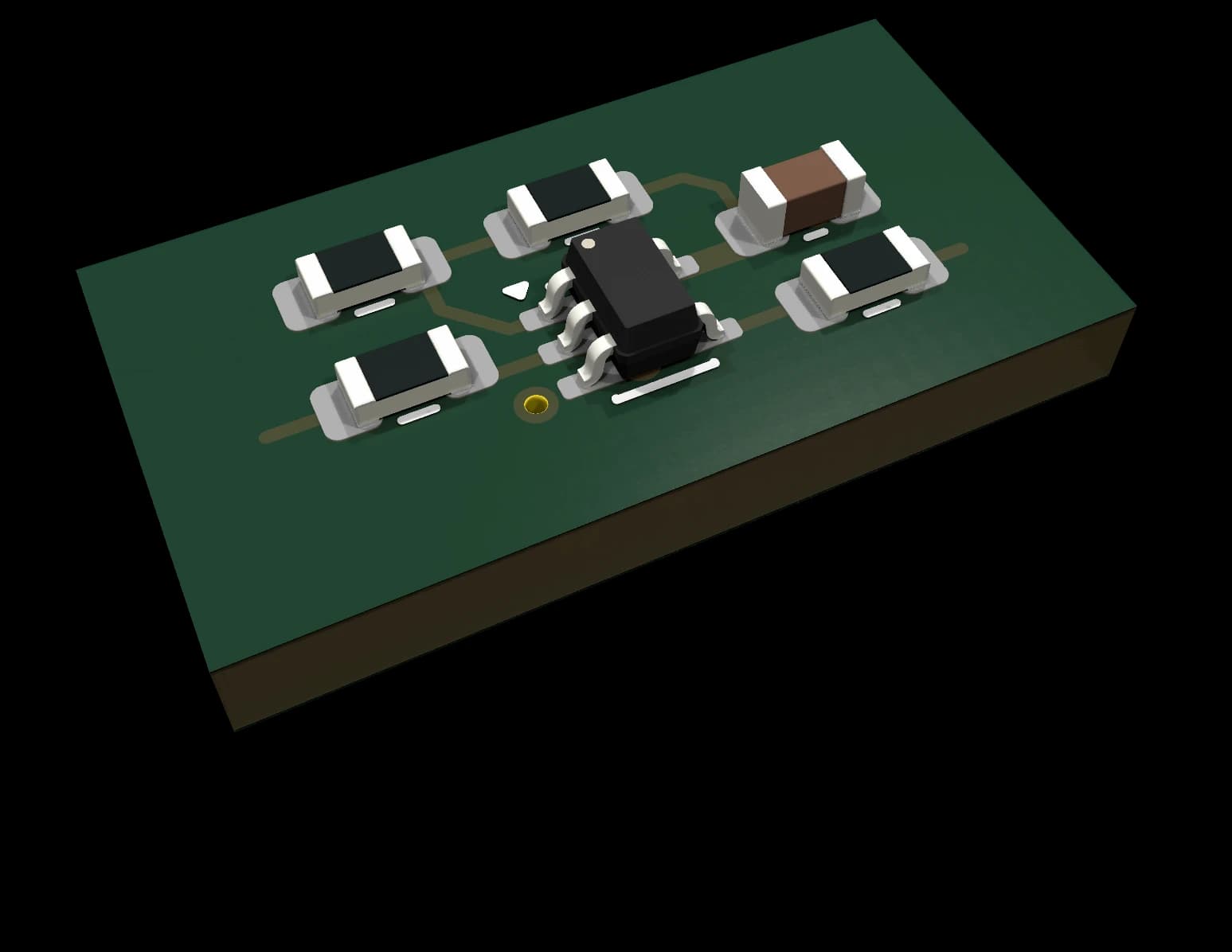
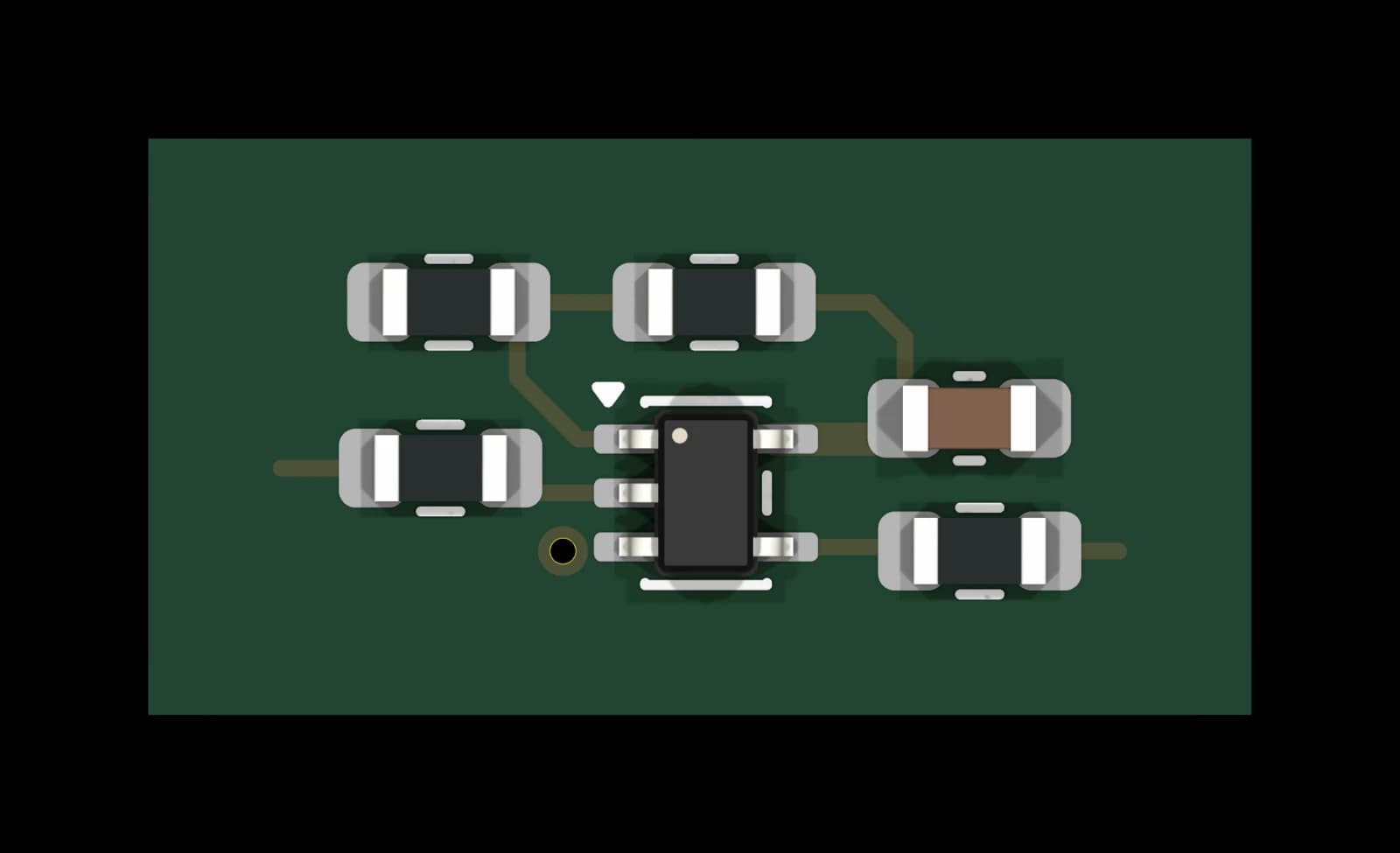
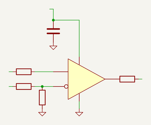
Key specifications
- Supply 4.5–5.5 V
- One channel, unidirectional, up to about 100 MHz
- TTL input threshold: 3.3 V logic drives it with margin
- Output enable by resistor option (always on by default)
Design notes
- One direction only (3.3 V → 5 V). For a bidirectional UART use 0165.
Seen in real hardware
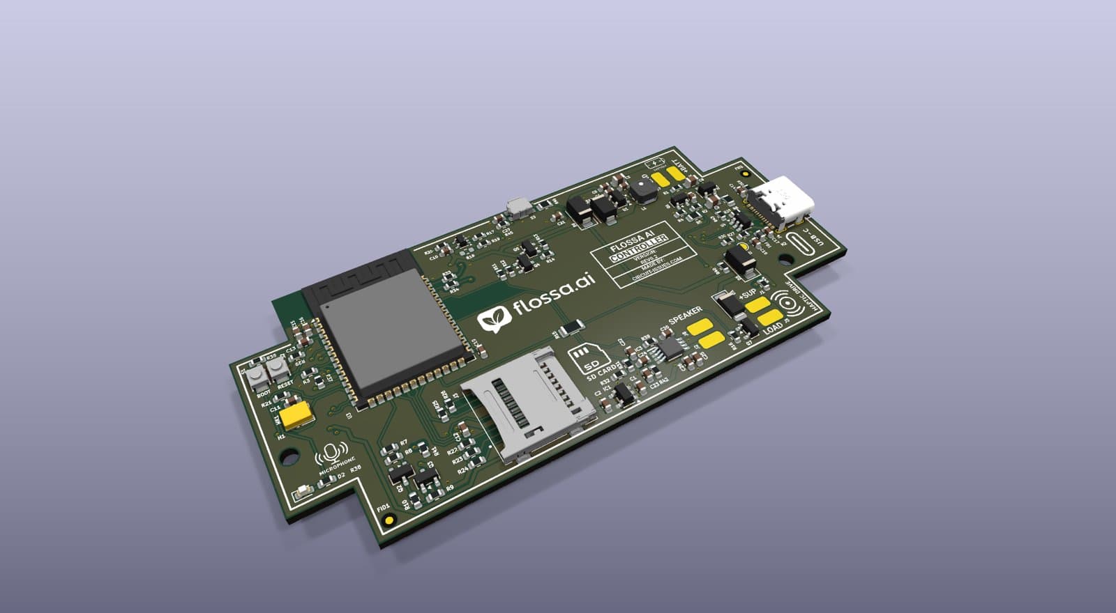
This block is not available yet. It is released once its checks are complete. Planned price: €29.
Planned package contents
KiCad 10 design block
Schematic and PCB layout fragment; symbols and footprints embedded
BOM (CSV)
Manufacturer part numbers and LCSC codes
Schematic PDF + README
Interface, specs, population options and design notes
3D models
STEP models of the special parts; standard parts use KiCad’s 3D library
template.yaml
Machine-readable interface and limits
PCB Composer
Get blocks like this one composed and routed into one board for your device, without opening KiCad. Quote within 24 h.
About PCB ComposerDevelopment status
| Block ID | 0040 |
|---|---|
| Block name | 0040-level-translator-3v3-to-5v |
| Version | 1.0 |
| Status | DRC clean – Schematic and layout pass the KiCad rule checks; not yet verified on hardware. |
| Open review items | None |
| PCB layout | Rule-checked layout fragment |
| Format | KiCad 10 design block (schematic + PCB) |
| Last change | 2026-11-03 |
Interface
Hierarchical labels the block exposes to the rest of your design. ${ID} is replaced per instance, so several copies can live on one sheet.
| Net | Direction | Description |
|---|---|---|
| VDD | Power in | 5 V supply of the buffer |
| TRANS_IN_${ID} | Input | 3.3 V logic input, series resistor |
| TRANS_OUT_${ID} | Output | 5 V logic output, series resistor |
FAQ
Which KiCad version do I need?
KiCad 10. The files are saved in the KiCad 10 format and are meant to be placed with KiCad’s Design Blocks feature (schematic block, then “Apply Design Block Layout” on the PCB).
Do I need the Circuit Issues part library?
No. Symbols are embedded in the schematic and footprints in the PCB, so the block opens on its own. Parts carry manufacturer part numbers and LCSC codes.
Is the layout production-ready?
The layout fragment passes the KiCad design rule check. Route it into your board and run DRC with your own fab rules.
Can I use the template in a commercial product?
The licence terms are published together with the first release.
Related templates
0050 Addressable RGB LED, Side View
KiCad 10 design block: side-emitting addressable RGB LED, WS2812-type 800 kHz protocol, 3.7–5.5 V, with data out for chaining.
DRC clean0140 ESP32-S3 Core (WROOM-2)
Free KiCad 10 design block: ESP32-S3-WROOM-2 (16 MB flash, 8 MB PSRAM) with native USB-C, ESD protection, BOOT/RESET buttons and 22 GPIOs on labels.
DRC clean0141 ESP32-S3 Core (MINI-1)
KiCad 10 design block: ESP32-S3-MINI-1 (8 MB flash) with native USB-C, ESD protection, BOOT/RESET buttons, I²C, UART and 25 GPIOs on labels.
Designed